I've been looking for internships for a while, mostly all of them require that you either study in or have the citizenship of the country in which the opportunity exists (mostly in US, Canada, and EU).
What can I do as a foreign student who wants to get a chance in such a field, especially that neither my uni or country overall offers a lot of opportunities for us?
I have been working with FPGAs for just about 10 years now. And I just realized that I have never done a CDC FIFO. Well... Maybe back in uni as some paper exercise.
It's such a weird gap too. Since it's like the first answer anyone gives whenever you want to transfer a lot of data across clock domains. But I just haven't needed a hardware FIFO for that yet.
So I spent the afternoon implementing one from scratch and shoving every edge case I could think of at it. Just as a learning exercise.
Have you found any weird gaps in your own knowledge?
I have the OA for the NVIDIA hardware internship at my college on October 22; can someone suggest the types of technical and aptitude questions asked, and as a BTech fresher, what kind of projects are sufficient?
I'm a third-year EEE student at UCL and I'm struggling to get past the initial application stage for FPGA internships. I rarely seem to receive online assessments and keep getting rejected after submitting my applications.
I'm particularly interested in FPGA engineering roles at trading firms, but I'm not sure whether the issue is my CV, lack of relevant experience, or something else.
For anyone who's been through this process, especially EEE students or people applying for FPGA/HFT internships, what helped you get more OAs? Is there anything specific recruiters look for at the CV screening stage?
I'm currently a student studying computer engineering and I was looking around for careers I could do with my degree.
I found out abt FPGA's later on and I really want to get into it.
The issue is that the engineering department in my school just started (I'm in the first set ever) so there's basically zero hardware-anything at all. I feel like it's so bad cause they've not even bothered to try to teach us any code in the last 3 years at this school.
Regardless I took it upon myself to learn something that will help me even a little when I finish from here and go do my masters, so I started with embedded and got an Arduino kit to start trying to learn with AI. I'm probably still very far off cause learning with AI isn't exactly ideal especially if it's a free version.
Joining this community has really opened my eyes to see how much farther the gap is and it feels like I'm in a hole trying to crawl out just to get to the base line
I'm curious how people doing FPGA work professionally actually spend their time, especially the parts of the workflow that are still frustrating.
Not looking for a generic "Vivado sucks" answer (although that's fair 😅). I'm more interested in specific examples.
A few things I'd love to hear about:
What part of your workflow consistently takes more time than you think it should?
What tasks do you find yourself doing manually or repeatedly?
What tools do you use day-to-day besides Vivado/Quartus/etc.? Editors, scripts, simulation, verification, CI, version control, internal tools, etc.
Are there any tools you've built internally because existing ones weren't good enough?
How do you handle Git/version control for RTL, constraints, IP, block designs, generated files, and tool projects?
What does debugging usually look like when something doesn't work?
Which parts of verification are the most painful?
How painful is moving between RTL changes → simulation → synthesis → implementation → hardware debugging?
Are there parts of working with constraints/timing that you wish had better tooling?
Do you use AI tools like Claude, ChatGPT, Copilot, Cursor, Claude Code, etc. for FPGA work? If so, what are they actually useful for?
Where have AI tools been useless or actively dangerous? Where have they been good?
If you could magically fix one part of the FPGA development workflow, what would you fix?
I'm especially interested in answers from people working on production FPGA designs, but hobbyist/academic perspectives are welcome too.
Would also love to know roughly what kind of FPGA work you do (industry/domain, team size, Xilinx/Altera/Lattice/etc.) since I imagine the pain points vary quite a bit.
I'm working on a Zynq UltraScale+ RFSoC design the RFDC ADC stream (128-bit TDATA, 8 × int16 per beat, 309.5 MHz clk_adc0) goes through an AXI4-Stream Clock Converter into an AXI DMA. The DMA side runs on a separate clock domain from a clk_wiz output.
I put ILAs on both sides of the converter to check data integrity on a 128-beat (1024-sample) burst delimited by TVALID/TLAST. At that time the output side ran at 100 MHz, i.e. about 3× slower than the input.
What I have saw
Input side: 128 contiguous valid beats in 0.41 µs, with tready never deasserted during the burst.
Output side: the same 128 beats come out contiguously at 100 MHz (1.28 µs), and TLAST is on the last beat.
A sine fit on both captures gives the same frequency, amplitude and residual, so no beat or samples seems lost or duplicated.
So the converter's FIFO must have absorbed the burst, with a peak occupancy of roughly 87 beats, which means a depth of at least that. Now I'd like to know exactly how deep it is.
Does anyone know the actual FIFO depth of axis_clock_converter? Is it a fixed value, or does it depend on parameters such as the clock ratio, the synchronization stages or the data width?
Is the depth user-configurable (a CONFIG. property, a hidden GUI option, an HDL parameter)?
I'm asking because I want to know the maximum size length I can capture without losing samples
I made a working correlator receiver in VHDL for my basys3 that can read from a raw IQ .bin file captured by an RTL-SDR and decode and display airplane positions and information. I want to make it work in real time and not just simulations but im having trouble figuring out how i can get the RTL-SDR stream to the basys3 without doing all of the signal detection on a pc first.
From what i understand the basys3 uart maxes out at 1 Mbps but adsb raw IQ sampling needs at least 32 Mbps. This is my second project on the basys3 and i dont have any other hardware but im open to any (cheap) suggestions that make this as little pc dependent as possible.
Quiero ver los proyectos de algunos usuarios para saber cuál experimentar primero, soy muy principiante pero me gustaría que se puede hacer más con las FPGA que no he encontrado en Youtube
I'm the developer of SILICON, a free and open-source digital circuit simulator written in C++ using Qt6.
It's going to become my Bachelor Thesis (I'm studying Computer Engineering @ Genoa Italy) and we are exeperimenting with It in the digital design course at my university (UniGe).
SILICON aims to provide a modern environment for designing and simulating digital circuits, primarily for educational purposes (like LogiSim), while gradually incorporating more advanced EDA capabilities.
Some of its current features include:
• Graphical circuit editor with logic gates, arithmetic components, flip-flops, registers, ROMs, and more.
• Event-driven digital simulation with multi-bit buses and four-state logic.
• Live waveform visualization and input waveform editing with FST firstclass support.
• Verilog import/export through Yosys integration.
• Automatic circuit placement.
• Reusable subcircuits and multi-document projects.
• Integrated code and binary editors, along with experimental ISA tooling.
• WASM web build
I'd especially appreciate feedback about the user interface, simulation behavior, missing features, and any bugs you encounter.
If you want to contribute as a dev send me a DM. I especially need help with MacOS support and Windows packaging.
Like companies claim to be MNC type idk exact but they show semiconductor related work and all but the website shows the training but the openings were for freshers like VLSI engineer/Associate vlsi Engineer. So does anyone know about company?
I have been thinking if a single end high speed tranceiver port on the high end FPGA's would be more practical than diff port now that microcoax and connectors are commonly available.
I guess the advantage of diff signaling is not that great if you have access to proper shielded microcoax cables. And diff at these speeds does not travel well on standard PCB stacks.
If you look at the wiring inside laptops, the diff >5.4Gbps lanes travel in diff mode through separate length matched microcoax wires, and I am thinking maybe that is a waste of one wire all the way from source to sink. They do send Wifi RF signals through single end so why not high speed on FPGA ports?
I use AI agents in my RTL work daily (both for ASIC design and FPGA prototypes). Modern LLMs are quite capable: they can implement complex features and find tricky bugs in large codebases. But the model is only half of it. The other half is the harness: the environment the agent works in and the tools it gets. Since early 2026 I have been experimenting with different parts of the harness, trying to make agents perform better. In this post I want to show what I was able to achieve: how a harness helps an agent investigate, reproduce and fix a hard bug in a large, real SoC.
Setup
I didn't want a toy. I wanted a large, real RTL codebase, so I picked Caliptra, the open-source hardware root of trust. It's big, well written, and backed by serious companies. It also runs on FPGA: upstream keeps a Vivado flow for the VCK190. This post stays in simulation, where the debug loop is the same whatever the target.
For the agent I used Anthropic's mid-tier model, Sonnet 5.5. It's a good balance of cost and brains, which is why a lot of people actually run it.
Then I needed a bug. Finding one hard enough took longer than I expected. I screened about 16 candidates: historical upstream fixes reverted back into the tree, plus a few still-open issues. An agent found every one of them just by reading the code, usually within a few minutes, without running a single simulation. Good news for agents, useless for an experiment.
The bug that survived is a real historical fix in the VeeR EL2 core (the RISC-V CPU inside Caliptra) that I put back into the tree. Upstream fixed it in the VeeR EL2 1.4 release in 2021; the release notes list it as "Store data collision with DCCM DMA error when address is 0x0".
The bug
The agent got an issue-style bug report. The short version:
Early in boot, the firmware recomputes a digest over its own ROM image and compares it with a constant fixed at build time. Normally the check passes. In one case the digest comes out wrong, even though the ROM is unchanged and the constant is correct. No fault, no exception, no ECC event, fully deterministic. The trigger is a coding pattern: the failing routine reads ROM word by word and, in the same tight loop, writes partial results to a scratch buffer in DCCM. Keep the accumulator in registers, or move the buffer out of DCCM, and the digest is correct. Only the first word of the ROM input looks corrupted.
Find and fix the RTL root cause. Add a test that reproduces the problem and passes after the fix.
What's actually going on: the core's load/store unit has store-to-load forwarding, and one guard condition is missing (el2_lsu_bus_intf.sv, the & lsu_busreq_r term). Without it, a store to DCCM wrongly forwards into a following load from ROM address 0. The load returns 0x0 instead of the ROM word.
Finding the fix isn't the hard part. Both arms of the experiment usually pointed at the right line of RTL within 5 minutes, just by reading. The hard part is the second half of the request: writing a test that fails on the buggy design. Two traps make that harder than it sounds:
The test template marks ROM as a side-effect region, and that disables forwarding. Write the obvious test and the bug never fires.
Code fetched from uncached ROM is slow, so the store and the load never meet in the pipeline.
So most of each run goes into getting a test to fail: build, simulate, look inside, change the test, repeat. That loop is where tools matter.
The experiment
Two arms, identical except for the harness:
Agent: Claude Code 2.1.289, Sonnet 5.5, medium effort.
Same everything else: same prompt, same container image, 8 CPUs, 10 GB RAM, a 90-minute wall-clock limit, no access to the internet. Caliptra at commit e379800c.
Without harness: the agent gets the repo and a shell. Caliptra's own Makefiles and test scripts are all there.
With harness: the same repo plus the harness, described next.
I ran 10 trials in each arm, numbered b1 to b10; trials with the same number form a pair.
The harness
The harness in this post is Booley, an open-source Python framework I'm building for agentic RTL work. Besides simulation and lint it has an FPGA implementation flow (synthesis through place and route in Vivado), though this experiment only needed simulation. The runs used the published 0.3.0 release.
What the agent gets on top of a plain shell:
Asimtool. It's a universal interface between the agent and the simulator. It works with different simulators (Verilator and Icarus Verilog today, commercial ones in progress), and it manages build reuse, trace creation and coverage. The interface stays the same in every project. What mattered most in this experiment is how it waits: the call blocks until the job finishes and returns pass or fail. If the job runs longer than four minutes, the agent gets a run ID and calls booley_poll, which blocks again and returns the moment the job exits. No guessing how long to wait.
B-Wave, a custom binary written in Rust that lets agents query waveforms directly. A simulation run with tracing on records a waveform, and the agent asks it questions: list signals, find the first cycle where a condition holds, print a few signals over a window of cycles as a text table, etc.
The build system is part of the harness. Caliptra's sources, simulator flags and firmware build are described once, in FuseSoC core files and a test list. The agent never touches Caliptra's Makefiles or the environment variables they expect. The no-harness agent has a build system too: those Makefiles, which it has to figure out on its own.
The Caliptra project setup used in this experiment: booley-prj-caliptra. Its README walks through the setup. Use it to play with Booley on Caliptra, or to rerun this experiment: revert the VeeR fix linked above and give your agent the bug report from "The bug".
Results
Both arms fixed the bug 10 times out of 10. With the harness the mean was 21.3 minutes. Without it, 55.8 minutes. Medians: 21.4 versus 53.3.
Three harness features account for most of the difference. Here they are, one by one.
Factor 1: seeing inside the design
When a test doesn't fail the way you expect, you need to see what the pipeline is doing. Without the harness, the agent does what we all did before we knew better: add $display, rebuild, rerun, grep. In pair b3 it went around that loop seven times, at about 6.5 minutes per rebuild. That's 37.8 minutes spent looking at signals.
With the harness, the agent built once with tracing on and asked the waveform 16 questions: 9.8 minutes in total.
Here's what those questions look like, from trial b1 (equivalent command lines, output trimmed). The agent's test kept passing on the buggy design, so it asked when the suspicious address match fires:
A ROM load matches a store that isn't even on the bus: that's the bug. But the load is flagged as side-effect, so the forward is cancelled and the test passes anyway. The agent changed the test's memory-attribute setting, and half a minute later the test failed on the buggy design.
(The long orange tail of the no-harness run, from 47 to 85 minutes, is its final tests running one after another. It has nothing to do with waveforms.)
Over all ten pairs the waveform saving averages 9.4 minutes.
Factor 2: getting the build to work at all
Caliptra's simulation Makefiles expect environment variables that aren't documented anywhere obvious (CALIPTRA_AXI4PC_DIR, CALIPTRA_PRIM_ROOT and friends). All 10 no-harness runs hit them. Most recovered within a few minutes.
Pair b1 shows how badly it can go. From 3.9 to 10.3 minutes the build failed three times while the agent hunted down variables. Then it exported them, but exports don't survive between the agent's shell calls. The next step quietly failed to build program.hex, and the simulation, with no program to run, hung until its timeout. That happened three times: 17.6 to 37.0, 60.8 to 65.9 and 66.4 to 71.5 minutes. At 71.5 the agent finally wrote a run.sh that set everything in one place. Total spent on setup: 36 minutes (30 minutes counting strictly).
With the harness, none of this can happen, because the build is part of Booley rather than something the agent assembles in a shell:
No Makefile variables to hunt. Booley drives the build through FuseSoC. The paths those variables point to were resolved once, when Caliptra was set up for Booley, and written into its FuseSoC core files. The agent never sees them.
No shell state to lose. Every sim call is self-contained. The per-test firmware build (program.hex and friends) is a declared step that Booley runs right before each simulation, with everything it needs.
No silent hangs on a missing program. If that firmware build fails, Booley reports the test as failed, with the build error, instead of starting a simulation with nothing to run.
The b1 harness run spent zero minutes on setup. Averaged over all ten pairs it's only 3.6 minutes, because nine of them recovered quickly. b1 is what the tenth looks like.
Factor 3: waiting on jobs that are already done
This one is a bit embarrassing for Anthropic, but I am going to report it anyway. Without a harness, the agent starts a build in the background and then guesses how long to wait. In b10, at 4.3 minutes, a build failed after one second. The agent had already run sleep 540 and didn't look again until 13.4 minutes. It did this four times in that run, sleeping through 30.7 of its 60 minutes.
With the harness, the tool call returns when the job is done. The b10 harness run took 13 minutes in total.
Across all ten pairs this is the largest factor: 11.2 minutes on average, and it mattered in 6 pairs. It's also a lower bound, because I counted only sleeps I could pin to a job that had demonstrably finished.
Summary
Same model, same bug, same prompt. With the harness, Sonnet 5.5 fixed it in 21 minutes on average; without it, in 56. The difference was in everything around that: seeing inside the design without a rebuild per question, a build that works on the first call, and getting the result the moment the job ends. On a hard RTL bug, most of the work is getting a test to fail, and that work runs on tools.
Disclaimers
The harness helps most on hard bugs
Smarter models benefit less
The sample is small: 10 trials per arm, one model, one bug, one SoC.
I built the harness, so weigh my enthusiasm accordingly.
spent last week building a raycasting renderer from scratch in systemverilog! got it working in verilator with c++/sdl visualization.
i implemented ray generation, dda-based grid traversal, wall detection, distance calculation, and pixel generation. i then used verilator for simulation and a c++/sdl program to visualize the rendered output.
my priority was getting the raycasting logic working, so code cleanup took a back seat. i'm wrapping up for now to focus on other work, but hope to revisit it later to clean up the rtl and explore an fpga implementation.
I'm considering buying a Digilent Nexys 2 for my project to learn fpga from scratch real-time Sobel edge detection on FPGA using an OV7670 camera and VGA output.
Would this board still be suitable for this project in 2026? Any compatibility issues or advice from people who have used it? Is it so ancient?
I found it online for only $30 idk if i shpuls buy
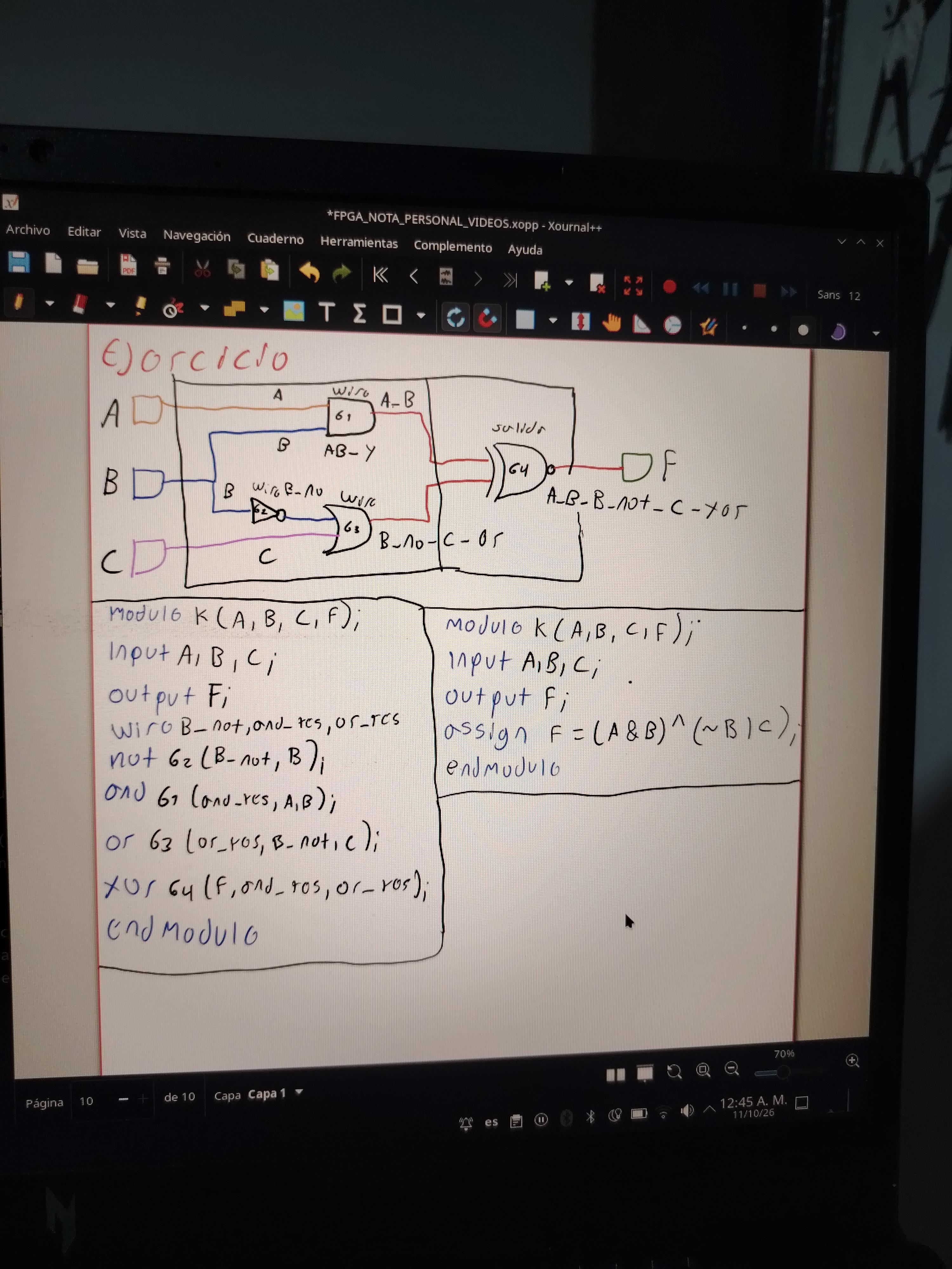
Después de pasar tanto tiempo pensando por dónde empezar a aprender FPGA, finalmente decidí comenzar con un video educativo en español. Este video enseña Verilog desde cero y explica los conceptos fundamentales.
Elegí Verilog porque me pareció más accesible y porque parece requerir menos contacto con conceptos en inglés que otras opciones de HDL.
Este fue el primer ejercicio y, ¡realmente me resultó difícil! Analizar el circuito compuerta por compuerta me tomó mucho tiempo, mientras que entenderlo mediante la lógica binaria me resultó mucho más fácil.
Por ahora, ya he descubierto que muchos conceptos de la programación FPGA se pueden relacionar con la programación de software.
Sin embargo, este ejercicio me permitió aprender bastante. Lo hice sin utilizar IA y dividí el circuito en dos partes para comprenderlo mejor. De esta manera, pude analizar más fácilmente la estructura del circuito y las relaciones lógicas entre las señales.
En cuanto a `wire` y `assign`, entenderlos fue bastante sencillo e intuitivo.